PART/ mag.x 125
Mag.x 125 Weitwinkel-Mikroskopsystem
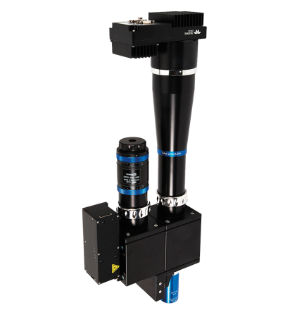
Das Weitwinkel-Mikroskopsystem Optem® mag.x 125 stellt eine neue Klasse optischer Systeme dar, die mikroskopähnliche Auflösung mit weiten Sichtfeldern kombiniert, um moderne hochauflösende Sensoren mit einem Durchmesser von bis zu 57 mm zu unterstützen. Its enhanced autofocus capability delivers exceptional speed, precision, and reliability for advanced metrology and inspection applications. The fully modular design can be configured for a wide range of applications, from a straightforward optical system without illumination to a fully featured configuration incorporating coaxial illumination and closed-loop autofocus.
High-speed, high-precision autofocus capability
The Optem mag.x 125 widefield microscope system features an updated autofocus sensor and focus actuator hardware, delivering fast, precise, and repeatable performance for demanding inspection and metrology applications. Designed for high-throughput inspection of flat-panel displays, wafers, and advanced packaging, the system combines rapid focus tracking with nanometer-level Z-axis positioning to maintain image quality, measurement accuracy, and throughput.
Modular design for high-resolution imaging
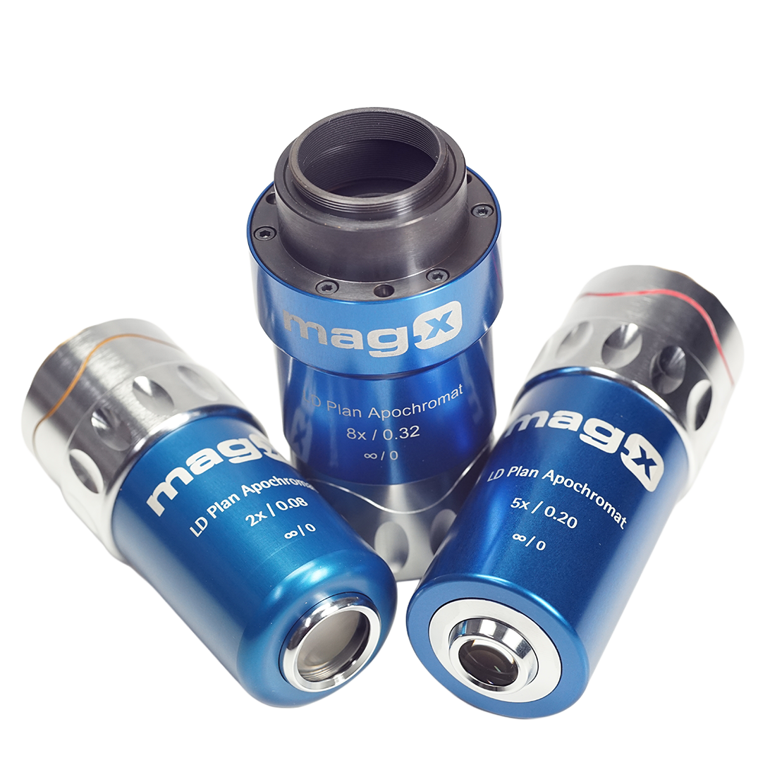
High-resolution inspection applications demand flexibility, precision, and seamless integration. The mag.x 125 system offers a fully modular platform that can be easily integrated with a wide range of objective lenses, tube lenses, illumination tubes, autofocus modules, mounting plates, and other accessories to meet specific application requirements.
| Objective Lens - Plan Apochromat | Tubuslinsensystem | |||||||||||||||
| Mtub : 1x | Mtub : 2.25x | |||||||||||||||
| f'tub : 250 mm | f'tub : 563 mm | |||||||||||||||
| 2y' : 25 mm | 2y' : 56.3 mm | |||||||||||||||
| Magn./NA | WD | f'obj. | δ obj | R0 | M | 2y | NA' | R'0 | M | 2y | NA' | R'0 | ||||
| mm | mm | µm | lp/mm | mm | lp/mm | mm | lp/mm | |||||||||
| 2x/0.08 | 24 | 125,0 | ± 42,7 | 293 | 2,0 | 12,5 | 0,04 | 147 | 4,5 | 12,5 | 0,018 | 65 | ||||
| 5x/0.20 | 13 | 50,0 | ± 6,8 | 733 | 5,0 | 5,0 | 0,04 | 147 | 11,25 | 5,0 | 0,018 | 65 | ||||
| 8x/0.32 | 23 | 31,3 | ± 2,7 | 1172 | 8,0 | 3,1 | 0,04 | 147 | 18,0 | 3,1 | 0,018 | 65 | ||||
NA Numerical aperture in the object space; NA=n * sin (σ)
WD Working distance
f'obj Focal length of the objective lense
f'tub Brennweite der Tubuslinse
δobj Depth of field at 546 nm; δobj = ± n * λ/(2*NA2)
R0 Cut off frequency in object space at 546 nm; R0 = (2*NA) / λ
R0' Cut off frequency in image space at 546 nm; R0' = R0 /M
2y' Image field size (maximum detector diagonal)
2y Object field size
M Magnification of the overall system; M = Mobj * Mtub
Präzise Technik mit innovativem optischem Design
Exact telecentricity on both the object and image sides
Diffraction-limited optical performance across the complete image circle
Präziser und dynamischer Autofokus
Modular, configurable architecture for easy system integration
Halbleiterinspektion und -verarbeitung
Flat-panel display processing (TFT and OLED)
Printed circuit board (PCB) processing
Micro measurement and metrology
Fluoreszenzmikroskopie
Digitale Pathologie
| Objective Lens - Plan Apochromat | Tubuslinsensystem | |||||||||||||||
| Mtub : 1x | Mtub : 2.25x | |||||||||||||||
| f'tub : 250 mm | f'tub : 563 mm | |||||||||||||||
| 2y' : 25 mm | 2y' : 56.3 mm | |||||||||||||||
| Magn./NA | WD | f'obj. | δ obj | R0 | M | 2y | NA' | R'0 | M | 2y | NA' | R'0 | ||||
| mm | mm | µm | lp/mm | mm | lp/mm | mm | lp/mm | |||||||||
| 2x/0.08 | 24 | 125,0 | ± 42,7 | 293 | 2,0 | 12,5 | 0,04 | 147 | 4,5 | 12,5 | 0,018 | 65 | ||||
| 5x/0.20 | 13 | 50,0 | ± 6,8 | 733 | 5,0 | 5,0 | 0,04 | 147 | 11,25 | 5,0 | 0,018 | 65 | ||||
| 8x/0.32 | 23 | 31,3 | ± 2,7 | 1172 | 8,0 | 3,1 | 0,04 | 147 | 18,0 | 3,1 | 0,018 | 65 | ||||
NA Numerical aperture in the object space; NA=n * sin (σ)
WD Working distance
f'obj Focal length of the objective lense
f'tub Brennweite der Tubuslinse
δobj Depth of field at 546 nm; δobj = ± n * λ/(2*NA2)
R0 Cut off frequency in object space at 546 nm; R0 = (2*NA) / λ
R0' Cut off frequency in image space at 546 nm; R0' = R0 /M
2y' Image field size (maximum detector diagonal)
2y Object field size
M Magnification of the overall system; M = Mobj * Mtub
Präzise Technik mit innovativem optischem Design
Exact telecentricity on both the object and image sides
Diffraction-limited optical performance across the complete image circle
Präziser und dynamischer Autofokus
Modular, configurable architecture for easy system integration
Halbleiterinspektion und -verarbeitung
Flat-panel display processing (TFT and OLED)
Printed circuit board (PCB) processing
Micro measurement and metrology
Fluoreszenzmikroskopie
Digitale Pathologie