Architectural Considerations for Modern UV Curing in Electronics Manufacturing
 The Quarter 2 issue of UV+EB Technology magazine features an article by Excelitas Marketing Manager Stacy Hoge examining how UV and UV LED curing technologies are shaping the future of electronics manufacturing by enabling fast, low-temperature curing of inks, adhesives and coatings.
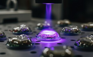
Hoge explores UV curing's expanding role across AI data center hardware, semiconductor packaging, display and mobile device modules, PCBs, high-capacity hard disk drives and fiber-optic and cable assemblies, where reliable, high-precision processing is essential to protecting sensitive components and maintaining throughput. She also details high-resolution printing applications for component identification, traceability and security features on optical and electrical cable films used in high-security infrastructure.
The article covers the key architectural and spectral decisions that determine system performance: spot versus area curing and narrow-wavelength UV LED sources versus broad-spectrum UV systems. Each approach involves distinct tradeoffs in precision, coverage, heat output and material compatibility that manufacturers must weigh against their specific application requirements.
Read the article, "Architectural Considerations for Modern UV Curing in Electronics Manufacturing," in UV+EB Technology magazine to learn how aligning curing architecture and spectral output with material and application requirements can help manufacturers achieve reliable, high-quality curing across a wide range of electronics processes.