Timing resolution and time walk in super low K factor single-photon avalanche diode—measurement and optimization
Abstract
Timing resolution (or timing jitter) and time walk are separate parameters associated with a detector’s response time. Studies have been done mostly on the time resolution of various single-photon detectors. As the designer and manufacturer of the ultra-low noise (ƙ-factor) silicon avalanche photodiode the super low K factor (SLiK) single-photon avalanche diode (SPAD), which is used in many single-photon counting applications, we often get inquiries from customers to better understand how this detector behaves under different operating conditions. Hence, here, we will be focusing on the study of these time-related parameters specifically for the SLiK SPAD, as a way to provide the most direct information for users of this detector to help with its use more efficiently and effectively. We will be providing the study data on how these parameters can be affected by temperature (both intrinsic to the detector chip and environmental input based on operating conditions), operating voltage, photon wavelength, as well as light spot size. How these parameters can be optimized and the trade-offs from optimization from the desired performance will be presented?
Introduction
Single photon counting technology has been growing significantly over the past three decades. In the earlier days, single photon counting was mostly experimental and used in many scientific research arenas, such as correlation spectroscopy, single molecule detection, and ultra-low fluorescence detection. More recent research in Lidar imaging and quantum communication also employs this technique.1 It had since moved onto many mainstream commercial applications, such as particle sizing, atmospheric aerosol Lidar, protein molecule analysis in drug development, and super resolution microscopy.
The basis of single photon counting technology lays in utilizing an ultra-low noise detector with high single photon detection efficiency (PDE). One such detector is the super low K factor (SLiK) silicon single-photon avalanche diode (SPAD). This SPAD has an active area diameter of 180 μm and is used to build one of the most well-known single-photon counting modules (SPCM), the SPCM-AQRH2 series. It can detect from single to several million photons per second, giving the detector module high dynamic range. It has very low dark noise, down to <10 counts∕s while having high single PDE especially in the 550- to 1000-nm wavelength range. Although these characteristics are very desirable in many photon counting applications, other parameters of the detector, such as timing resolution (TR) or time jitter, and time walk, have been sought after in some more advanced technologies, such as high resolution optical tomography, Lidar, fluorescence lifetime measurements for single molecule studies, and life cell microscopy.

TR and time walk are two essential factors associated with the precision of time measurement of the photon triggered output signal.
Time resolution is the statistical uncertainty or timing error that occurs when one attempts to measure the temporal start of the output signal of the SPCM. If the resolution was zero, every output pulse would occur at the exact same time from the original photon trigger event in the avalanche photodiode. However, due to variations in the avalanche process, as well as subtle effects within the electronics, there are always variations when the output pulse occurs. This error is the TR or timing jitter. It is also a function of wavelength and the location on the SPAD, where the avalanche breakdown is first initiated.
In measurement terms, time resolution is the multiple and repeated time measurement of the pulse from a SPAD after every photon event is detected. The time data is plotted on a statistical curve, from which the full width at half maximum (FWHM) is calculated.4 Figure 1 illustrates the definition of TR.
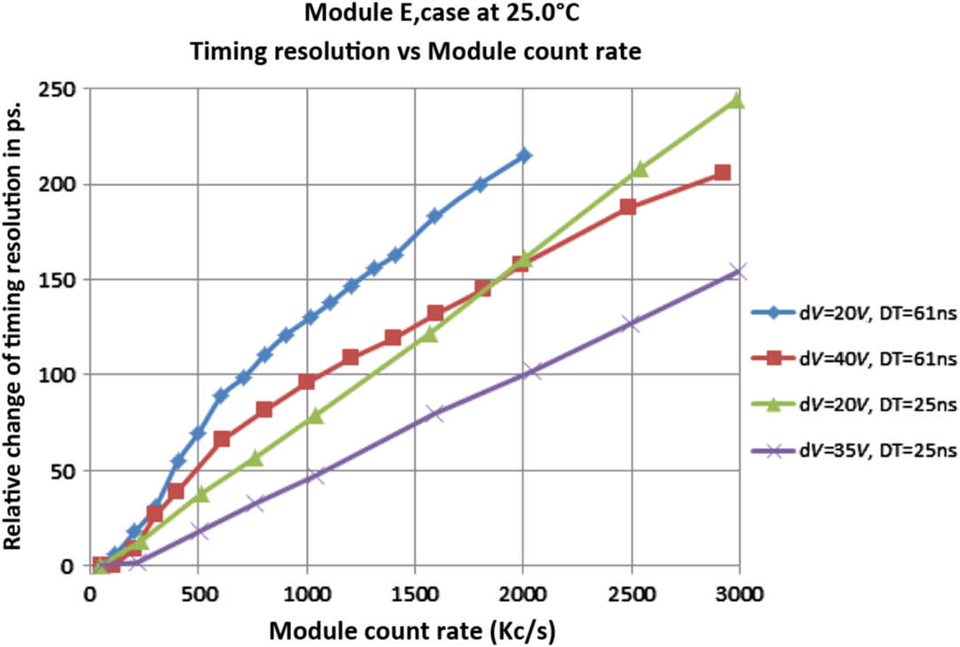
Time walk is the temporal shift of the output pulse of the SPCM module and is mainly due to the effects of avalanche diode self-heating at higher count rates and to a lesser extent, the electronics around the SPAD. In effect, the peak of the output pulse is shifted in time as the count rate increases. Figure 2 illustrates the definition of time walk.

Diode self-heating—at higher count rates, the thermal electric cooler (TEC) cannot evacuate the heat generated by the SPAD fast enough and temperature gradient will occur between the SPAD and the temperature monitoring circuit. The SPAD temperature will rise slightly causing the breakdown voltage to rise a little. Consequently, this will have an effect on the SPAD performance and will degrade the timing performance.
Many studies have been done on the SPCM by users of the module including studies on TR and time walk. As the SLiK SPAD has never been commercially sold separately from SPCM-AQRH module, there has been interest to understand the basic timing characteristics SPAD.
Experimental Setup
The experimental set up for measuring the TR is shown in Fig. 3. The default measurement is done at 825 nm. Measurements have also been done at 440 and 637 nm. The light sources used are the LDH series of pulsed laser diode heads from Picoquant, coupled to a multimode fiber with 100-μm core diameter and 140-μm cladding. The laser diodes are driven by the PDL800-B single channel laser driver from the same manufacturer as the laser diodes. The laser diode is driven at 2.5-MHz pulse rate, where ∼1% of the time a single photon is being detected by the SPAD.
As the laser beam intensity is too high for single photon detection, the output of the laser from the fiber is attenuated to reduce the probability of a photon striking the SPAD to around 1 in 100 laser pulses. An Ophir ND3 attenuator is used for most of the experiments
A 500-μm diameter pinhole follows the attenuator to channel the light into a 50∶50 beam splitter, where half of the photons are reflected back to a CCD camera for focus and position alignment for detector active area scanning, and the other half of the photons are transmitted through the objective of a microscope lens onto the SLiK SPAD. The light spot on the SPAD is 10 μm in diameter. The scanning of the active area of the SPAD for each single measurement point is done in 20 μm steps across the full active area surface. The SLiK SPADs are assembled in an active quenching circuit used in the standard SPCM-AQRH series for the test

For precise timing measurements, it is critical to properly synchronize the laser and the detector. To synchronize the laser signal to the SPAD output, an HP B1101A pulse generator, which functions as a programmable delay is programmed in which the pulser “START” is synchronized with the “SYNC” output of the laser driver. The output of the single photon counting detector is then channeled to an Ortec 566 time-to-amplitude converter (TAC), which is adjusted to time range of 50 ns. The output of the TAC is fed to the Ortec 926 analog-to-digital converter followed by a multichannel analyzer (MCA) for statistical data gathering and interpretation.
Measurement Assumptions and Definitions
The experimental data for this paper were done using the standard 825-nm pulse laser with FWHM of 80 ps, unless otherwise noted. The data presented here are based on 18 standard SLiK SPADs. In order to test the SLiK SPADs, they are mounted onto a standard Excelitas SPCM-AQRH series single photon counting modules. The measurement results therefore include the TR of the SPCM module electronics as well as the TR of the SPAD.
The pulse width of the laser also contributes to the FWHM of the measurement. However, this is not intrinsic to the SPAD and it is an external factor that has been compensated for in order to derive the final TR results. The laser pulse FWHM is quadratically subtracted from the MCA FWHM peak for all data measured:
where TRM is total measured timing resolution, TRL is total timing resolution from the laser source, and TRD is net timing resolution from the SPCM module.
Test conditions are in so-called “starved mode” such that TR is given for single photon. The accuracy of the TR measurement degrades significantly if the setup allows more than a photon per pulse. This is done in order to separate the time jitter of the module electronics from that of the SPAD itself. If the count rate of the SPAD is high (>1 Mcps), the TR of the SPAD is essentially reduced to 0 and one ends up measuring the TR of the electronics alone. For this SPCM model, the electronics’ timing jitter (Tr) is around 30 ps. So, combined with the overall module TR of 200 to 350 ps (including the SPAD), the contribution from the electronics is small. Most of the TR is due to the uncertainty in the SPAD avalanche process.
The TR is mainly a function of the electric field generated in the SPAD and, consequently, is a function of the breakdown voltage (Vbd) and the bias voltage (Vop). The SLiK SPAD is a super low ƙ APD (ƙ ∼ 0.002) meaning the ratio of ionizing electrons to ionizing holes is very large, and it is mostly the electrons that cause the avalanche to propagate through the junction under the field, generating collisions in which more electron hole pairs are released during the avalanche. How quickly and how many electrons accelerate through the junction will affect the TR of the SPAD. Also, the SLiK SPAD has a thicker junction than many other types of SPADs and combined with a larger active area means that it has a higher Vdb and Vop than other types of SPAD as well. See Fig. 4 for the structure of this SPAD. This gives the SLiK the advantage of having high PDE, especially at longer wavelengths.
Since TR is a function of the breakdown voltage, Vbd, and the operating voltage, Vop (given by the difference between the two as the excess or overvoltage: ΔV ¼ Vop − Vbd), any parameters that could affect the Vbr or the ΔV can affect the TR.
The TR measurement is defined for one photon. The light spot size is 10-μm diameter, centered in the active area. Tests are done by scanning the full detector active area in 20-μm steps for a full-scan mapping of the timing measurement. The laser is operated at 2.5 MHz.

Data accumulation time is 5 s at each 20-μm spot location throughout the full scan across the detector active area. The counting rate for the SPAD is 50 KHz.
The average FWHM of the 18 detectors is 392 ps, with a standard deviation of 57 ps. The breakdown voltage of these 18 SPADs range from 280 to 362 V.
Measurement Results
Timing Resolution versus Wavelength
TR tends to degrade in the shorter wavelengths (i.e., 400 nm) compared to longer wavelengths (>600 nm). The absorption of the photons in the first few hundreds of nanometers of the multiplication region is the main contributor to the TR of the SPAD. At shorter wavelengths, the photons do not penetrate very far into the silicon. So, when the avalanche is initiated, they have father to travel and there is more uncertainty in the avalanche path. UV is absorbed in the low field region, where the drift velocity is slower. It takes longer for the avalanche to complete (Fig. 5).
Timing Resolution versus Light Spot Position
TR degrades rapidly as the photon hits away from the center of the detector. Photons that are gathered farther from the high field region are accelerated at slower rates and so there is a larger spread on the TR. This is also likely because of the uniformity of the SPAD that is usually better toward the center of the chip, thus having a more uniform high field region, where electrons are accelerating at the same speed (Fig. 6).
Time Resolution versus Light Spot Size
Larger light spot size has slower TR than small spot size. This is generally because of the nonuniformity of the SPAD. So, if a photon impinges the SPAD in the same small area all the time (small spot size), the response time will be similar thus having short TR.

If a photon hits the SPAD at a different area over a larger spot size, with slightest differences in the high field region, the response time may be different, thus causing a wider spread in the FWHM measurement.
In this case, only 10- and 50-μm diameter light spot size was used in the experiments. In case of a perfectly uniform device, the spot size scanned would not make much of a difference in the TR. In reality, there is no such perfect uniformity in this type of SPAD device; hence there will always be slower TR when the light spot size increases.
Fig. 6 (a) Example of a TR scan data across the SLiK active area; (b) TR versus light spot position for module D; and (c) TR versus light spot position for module F.
All 18 modules have been measured using the two spot sizes. Here is the comparison data for 5 out of the 18 modules measured (Table 1).
Time Resolution versus Excess Voltage (or ΔV)
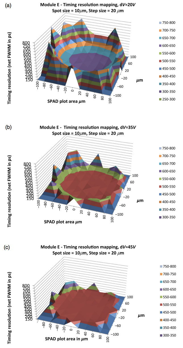
The difference between the voltage and the voltage above breakdown voltage in which the SPAD is operated at Geiger mode is termed the excess voltage or delta voltage (ΔV or dV). TR will improve as the ΔV increases. Higher operating voltage drives electrons faster as well as more electrons through the electric field. However, SPADs with low breakdown voltage tend to give better TR than SPADs with higher breakdown voltages since for a given ΔV, the SPAD with a lower breakdown voltage will have a stronger electric field, which helps to propel the electrons through quicker for the same ΔV.
For example, for a SPAD with a Vbr of around 350 V and operating at ΔV of 20 V, the TR is around 350 ps, whereas at a ΔV of 35 V, the same device could have a TR of around 250 ps. However, for SPAD with a Vbr of around 250 Vand a ΔV of 20 V, the TR could be around 300 ps and at ΔV of 35 V, the TR could be around 200 ps or lower.
With a greater ΔV, the area of the SPAD with the same low TR increases. In other words, the TR becomes more uniformly low across the full active area of the SPAD. Thus, at higher ΔV, the SPAD becomes uniform across the full active area both in improved TR and PDE (Fig. 7).
Time Resolution versus Case Temperature
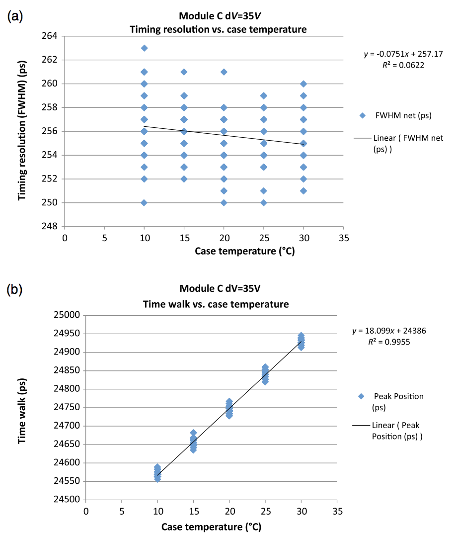
The TR varies very little with the change in case temperature at low count rates (i.e., 50 Kc∕s). This is because at low count rates, the SPAD has low self-heating and its temperature is accurately maintained by mounting it on TEC, even if the case temperature changes.
Time walk, on the other hand, changes significantly with the change in case temperature even at low count rate. As the case temperature changes, the circuit electronics will create time jitter that will overtake the SPAD’s constant TR at TE cooled temperature in shifting the output pulse peak.
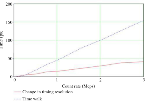
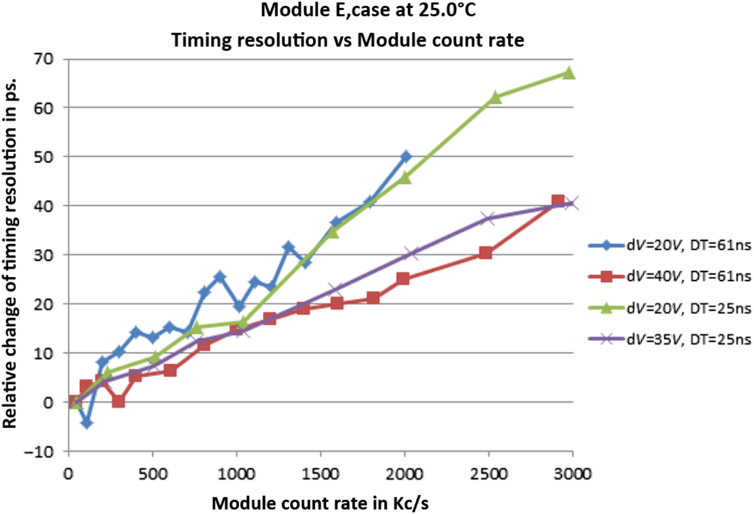
As the count rate increases, the peak position of the pulse shifts in time, creating time walk. The majority of the time walk is caused by the SPAD chips’ self-heating due to increased count rate and a small portion is due to electronics—so called instrument response function. Simulated time walk of a SLiK module with increasing count rate is illustrated in Fig. 8. An actual measurement sample is shown in Figs. 9–11.
Timing Resolution and Time Walk Optimization
Time resolution and time walk are important parameters for any applications using timecorrelated single photon counting technique. Examples of such include fluorescence lifetime measurements, fluorescence lifetime imaging, optical tomography or Lidar imaging, etc. The understanding of the contribution factors to the TR and time walk will make it easier to monitor and select an SPAD that can be tailored better to fit the timing requirements.
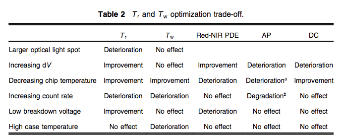
However, the optimization of TR and time walk of the SLiK SPAD comes with some trade-offs. By increasing the ΔV, for example, the dark count (DC) of the SPAD will increase while the TR will improve. Increasing the count rate to get more resolution or better system data will worsen the TR and by compensating with cooling the APD further in order to keep the TR down, there will be the risk of increasing the afterpulsing (AP).
Table 2 lists some of the major parameters of the SPCM on how they vary when optimizing TR (Tr) and time walk (Tw).
As shown in the above summary table, to get an improvement on Tr and Tw means there will be some trade-offs in other SPAD performance. For example, by increasing the dV to get better Tr, the AP and the DC of the SPAD will deteriorate while there will be an improvement of the NIR PDE at the same time. This will be very useful for applications, such as Lidar using NIR light source, since the signal will be strong so DC of the SPAD is not that critical, but having better NIR PDE will help. But if the Lidar is at green wavelength, for example, then it may be even better to consider a low breakdown voltage SPAD since that will not affect most of the performance criteria other than NIR PDE, which is not critical in this case.
Conclusion
The measurement of the SLiK SPAD’s TR and time walk has been discussed. Some of the SPAD’s timing characteristics have been presented against several influential factors, such as wavelength, light spot size, light spot position, operating voltage, count rate, and temperature in a limited fashion. This is not the fullest extent of characterization of TR and time walk for the SLiK, but it allows for sufficient awareness for the optimization and selection of the SLiKbased SPCM module for TR where there is a need.
