PART/ 85108076030
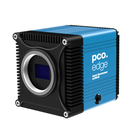
pco.edge 9.4 bi CLHS sCMOS Camera
 Powered by Bioz
The pco.edge 9.4 bi CLHS is our first sCMOS camera with photon counting capabilities for challenging and demanding microscope methods like Lightsheet Fluorescence Microscopy (LSFM) and Structured Illumination Microscopy (SIM). This sCMOS camera combines an extremely low readout noise of 0.3 e- with a quantum efficiency of up to 85% with a broad spectrum out to NIR. The sensor incorporates microlenses and a full pixel height deep trench isolation for crosstalk suppression, resulting in an excellent modulation transfer function. The camera provides a large image circle using a high-resolution 9.4MPixel image sensor with a square pixel size of 4.6µm. The camera is equipped with four CLHS FOL channels – all aligned in one compact plug – capable of transmitting up to 4.9 GByte/s.
With low readout noise values, the pco.edge 9.4 bi CLHS can capture light with photon counting sensitivity and use even the smallest signals to gain information about the imaged samples. With its image sensor diagonal of 21.6 mm the camera offers a large image circle suitable for a wide range of applications in microscopy. Due to its rectangular layout, the pco.edge 9.4 bi CLHS can also be used for two-color applications that use image splitters.
| Sensor Technology | sCMOS BSI |
| Resolution (H x V) | 4096 x 2300 |
| Pixel Size (H x V) | 4.6 x 4.6 |
| Sensor Diagonal | 21.6 mm |
| Peak Quantum Efficiency | 85.0 % |
| Peak Quantum Efficiency Wavelength | 500.0 nm |
| Global Shutter | false |
| Rolling Shutter | true |
| Global Reset | false |
| Operational Modes |
Slow Scan Medium Scan Fast Scan |
| Readout Noise RMS |
0.4 e- 0.5 e- 0.6 e- |
| Readout Noise Median |
0.3 e- 0.4 e- 0.5 e- |
| Fullwell Capacity |
7000 e- 6500 e- 6500 e- |
| Dynamic Range |
23300:1 16200:1 13000:1 |
| Dynamic Range (log) |
87.0 dB 84.0 dB 82.0 dB |
| Dark Current | 0.4 e-/s |
| Sensor Temperature (Dark Current Reference) | 10.0 °C |
| Frame rate (Full Sensor) |
30.0 fps 60.0 fps 122.0 fps |
| Dynamic Range A/D Converter | 16 bit |
| Thermo Electric Cooling | true |
| Forced Air | true |
| Liquid Cooling | true |
| Working Temperature Image Sensor |
adjustable: 0 °C to +25 °C calibration setpoint: +10 °C |
| Data Interface | Camera Link HS FOL |
| Included Lens Mount |
C-Mount F-Mount |
| Width | 90.0 mm |
| Length | 109.0 mm |
| Weight (kg) | 1.35 |
| Height | 95.0 mm |
| Part Number | 85108076030 |
- Brightfield microscopy
- Fluorescence microscopy
- Digital pathology
- Single molecule localization microscopy (SMLM)
- Light sheet fluorescence microscopy (LSFM)
- Selective plane illumination microscopy (SPIM)
- Structured illumination microscopy (SIM)
- Raman spectroscopy
- Calcium imaging
- Förster resonance energy transfer (FRET)
- Fluorescence recovery after photobleaching (FRAP)
- High-speed bright field ratio imaging
- High throughput screening
- Opthalmology
- Biochip reading
- Total internal reflection fluorescence microscopy (TIRF)
- 3D metrology
- Industrial quality inspection
- Wafer inspection
- Image intensifier imaging
- Intravital microscopy
- Inspection
- Material testing
- Biometrics
- In-vivo microscopy
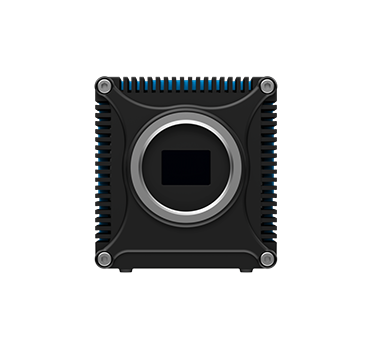
Front View
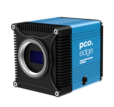
Front View 45 Degree
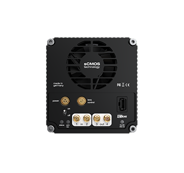
Rear View
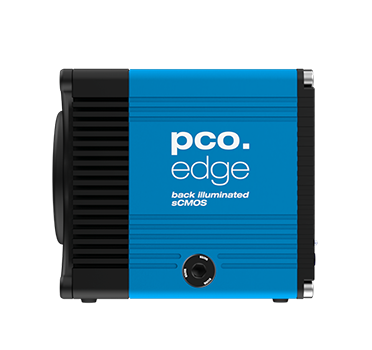
Side View
| Sensor Technology | sCMOS BSI |
| Resolution (H x V) | 4096 x 2300 |
| Pixel Size (H x V) | 4.6 x 4.6 |
| Sensor Diagonal | 21.6 mm |
| Peak Quantum Efficiency | 85.0 % |
| Peak Quantum Efficiency Wavelength | 500.0 nm |
| Global Shutter | false |
| Rolling Shutter | true |
| Global Reset | false |
| Operational Modes |
Slow Scan Medium Scan Fast Scan |
| Readout Noise RMS |
0.4 e- 0.5 e- 0.6 e- |
| Readout Noise Median |
0.3 e- 0.4 e- 0.5 e- |
| Fullwell Capacity |
7000 e- 6500 e- 6500 e- |
| Dynamic Range |
23300:1 16200:1 13000:1 |
| Dynamic Range (log) |
87.0 dB 84.0 dB 82.0 dB |
| Dark Current | 0.4 e-/s |
| Sensor Temperature (Dark Current Reference) | 10.0 °C |
| Frame rate (Full Sensor) |
30.0 fps 60.0 fps 122.0 fps |
| Dynamic Range A/D Converter | 16 bit |
| Thermo Electric Cooling | true |
| Forced Air | true |
| Liquid Cooling | true |
| Working Temperature Image Sensor |
adjustable: 0 °C to +25 °C calibration setpoint: +10 °C |
| Data Interface | Camera Link HS FOL |
| Included Lens Mount |
C-Mount F-Mount |
| Width | 90.0 mm |
| Length | 109.0 mm |
| Weight (kg) | 1.35 |
| Height | 95.0 mm |
| Part Number | 85108076030 |
- Brightfield microscopy
- Fluorescence microscopy
- Digital pathology
- Single molecule localization microscopy (SMLM)
- Light sheet fluorescence microscopy (LSFM)
- Selective plane illumination microscopy (SPIM)
- Structured illumination microscopy (SIM)
- Raman spectroscopy
- Calcium imaging
- Förster resonance energy transfer (FRET)
- Fluorescence recovery after photobleaching (FRAP)
- High-speed bright field ratio imaging
- High throughput screening
- Opthalmology
- Biochip reading
- Total internal reflection fluorescence microscopy (TIRF)
- 3D metrology
- Industrial quality inspection
- Wafer inspection
- Image intensifier imaging
- Intravital microscopy
- Inspection
- Material testing
- Biometrics
- In-vivo microscopy
Front View
Front View 45 Degree
Rear View
Side View
Subscribe Now!
Floating Web Forms block
Join the PCO Circular newsletter for early access to insights on our high‑performance imaging cameras. Receive the latest application notes, expert webinars, technical articles, educational videos, product innovations, and industry events designed for scientific, microscopy, research, and industrial imaging applications.
Floating Web Forms block